You will get A professional Schematic ,multilayer PCB Layout ,Gerbers and BOM files
Top Rated
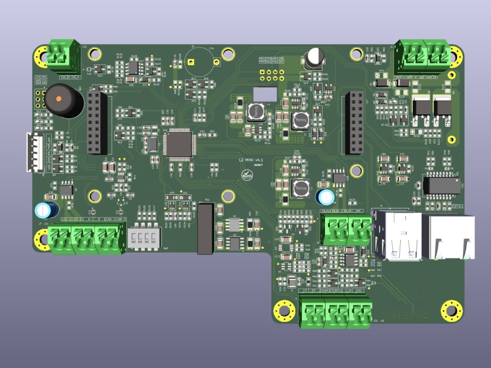
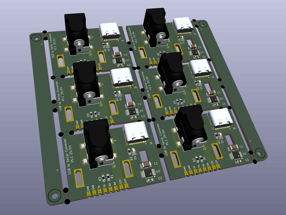
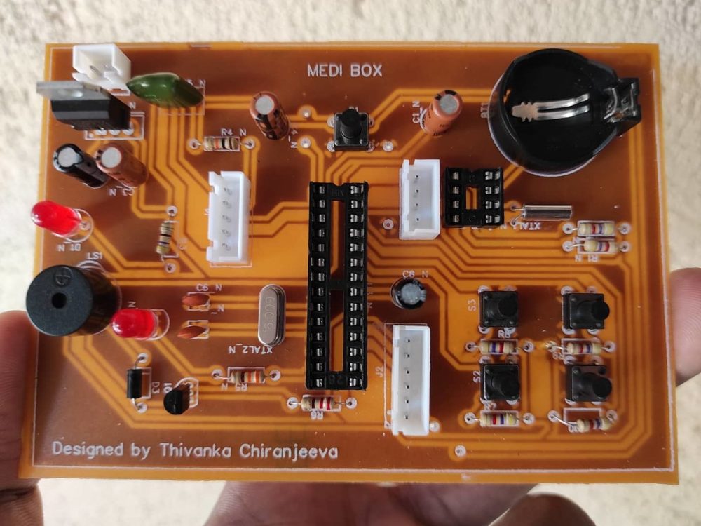
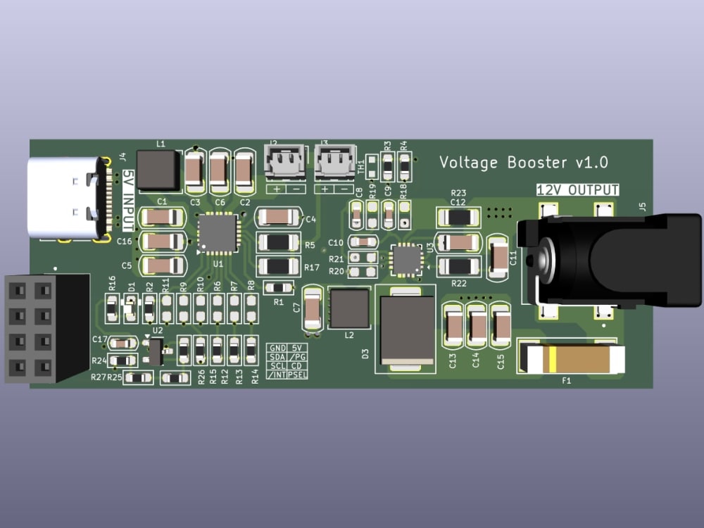
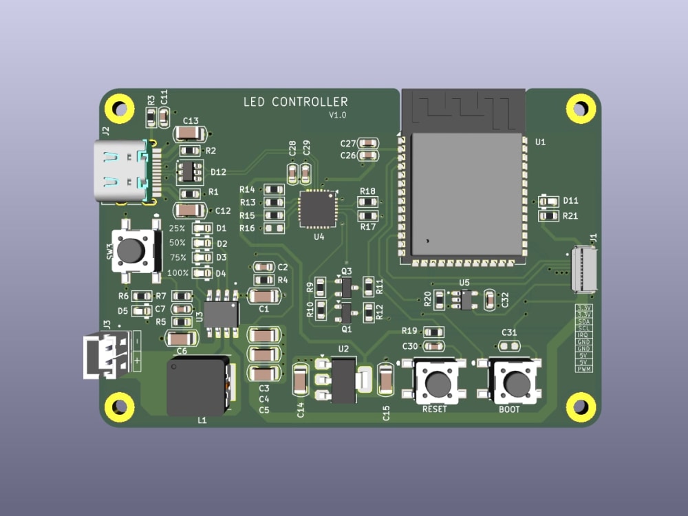
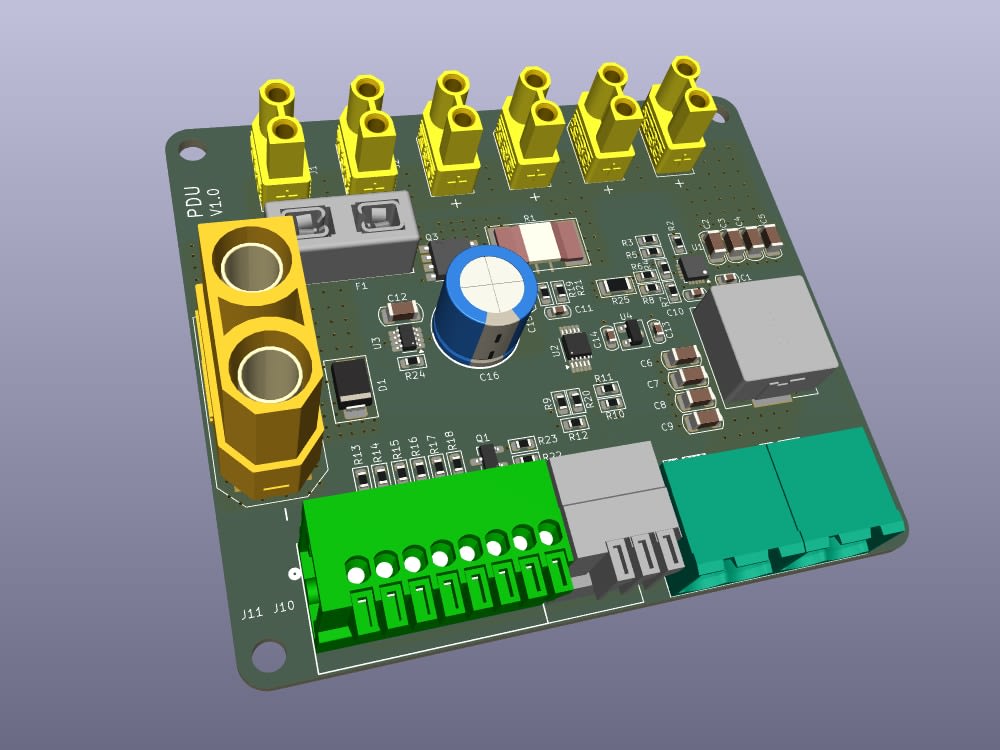
Top Rated
Project details
I’m Thivanka Chiranjeeva, an embedded systems engineer with 5 + years of hands‑on experience in schematic design and multi‑layer PCB layout, driven by a passion for transforming concepts into reliable hardware solutions. I excel in using KiCad, Eagle, and Altium Designer to deliver manufacturable, cost‑effective boards. My meticulous attention to DFM/DFT guidelines and version‑controlled workflows ensures that every design meets industry standards and client requirements. I thrive on collaborative problem‑solving, guiding clients from initial requirements through final deliverables with clarity, professionalism, and a commitment to on‑time delivery
Core Deliverables
Schematic Design - Analog & Digital Circuit Design
Multi‑Layer PCB Layout - 6+ layers, DFM/DFT‑compliant
Footprint & Library Creation - custom schematic symbols and PCB footprints
PCB Panelization - For efficient fabrication and assembly
BOM Generation - (vendor‑preferred parts, cost optimization) ([Upwork][9])
Gerber & CAM File Preparation - final fabrication outputs)
Why Choose Me?
Proven Expertise
Industry‑Standard Tools
Quality & Compliance
Structured Process
Collaborative Approach
Core Deliverables
Schematic Design - Analog & Digital Circuit Design
Multi‑Layer PCB Layout - 6+ layers, DFM/DFT‑compliant
Footprint & Library Creation - custom schematic symbols and PCB footprints
PCB Panelization - For efficient fabrication and assembly
BOM Generation - (vendor‑preferred parts, cost optimization) ([Upwork][9])
Gerber & CAM File Preparation - final fabrication outputs)
Why Choose Me?
Proven Expertise
Industry‑Standard Tools
Quality & Compliance
Structured Process
Collaborative Approach
Field of Expertise
Automotive, IoT, WearablesDesign Software
AutoCAD, Fusion 360, SolidWorks, OtherFile Format
JPG, PDF, SLDPRT, STEP, STLWhat's included
| Service Tiers |
Starter
$40
|
Standard
$80
|
Advanced
$150
|
|---|---|---|---|
| Delivery Time | 3 days | 5 days | 10 days |
Number of Revisions | 3 | 3 | 5 |
Number of Technical Drawings | 1 | 1 | 1 |
Concept Development | - | - | - |
3D Model | |||
Source Files |
Optional add-ons
You can add these on the next page.
Fast Delivery
+$20 - $50
8 reviews
(8)
(0)
(0)
(0)
(0)
This project doesn't have any reviews.
KA
Khalid A.
Jun 6, 2026
Flexible + Rigid PCB Design for LED + Capacitive Touch System with ESP32
AK
Atakan K.
May 21, 2026
Simple BLE beacon PCB, 35mm round, 7 components, JLCPCB-ready
Thivanka delivered a clean PCB design on time and was responsive to all questions. He clarified design decisions clearly and made updates promptly. Would hire again for future projects!
GS
Gabriel Aron S.
Apr 14, 2026
Schematic drawing of a linear PSU from the 90s
Fast and high quality work.
LE
Luke E.
Mar 5, 2026
PCB REV2 DESIGN OPTIMISATION
Thivanka is an expert in the field. He communicates clearly and ensures that the project meets the highest standards. I would recommend him to anyone and look forward to collaborating with him again in the near future.
LE
Luke E.
Nov 11, 2025
PCB Review and Optimization.
Thivanka is an exceptionally skilled PCB designer with extensive experience. He guided us through optimizing our design with expert insights and maintained outstanding communication throughout the process. We look forward to work with him again in the future.
About Thivanka
PCB Design Engineer | Multi-Layer Layouts | ESP32 & STM32 Expert
100%
Job Success
Kuliyapitiya, Sri Lanka - 3:27 pm local time
I am a professional Embedded Systems Engineer specializing in high quality schematic capture and PCB layout. Whether you need a simple 2-layer prototype or a complex multi-layer industrial board, I ensure your design is optimized for both performance and Design for Manufacturing (DFM) to keep production costs low.
Core Expertise:
✅PCB Layout: High-speed digital, precision analog, and power electronics (Multi-layer).
✅Hardware Integration: Extensive experience with ESP32, STM32, Arduino, and LoRa.
✅Schematic Design: Component selection, circuit simulation, and custom library management.
✅Manufacturing Files: Full production packages (Gerber X2, BOM, Pick-and-Place, 3D STEP).
✅Industry Tools: Expert proficiency in KiCad, Altium Designer, and Autodesk Eagle.
Why work with me?
✅ Manufacturing Ready: I don't just "draw" boards; I design them to be built according to IPC standards.
✅ Fast Turnaround: Clear communication and strict adherence to your project deadlines.
✅ Post-Delivery Support: I provide technical support until your board is successfully fabricated and assembled.
Let’s discuss your project requirements. Send me a message or click "Invite to Job," and I’ll provide a quick initial review of your concept!
Steps for completing your project
After purchasing the project, send requirements so Thivanka can start the project.
Delivery time starts when Thivanka receives requirements from you.
Thivanka works on your project following the steps below.
Revisions may occur after the delivery date.
Discuss and Confirm the Requirements.
Design the Schematic.