You will get ESP32-Based Multi-Interface LoRa Communication Device with Relay Control
Project details
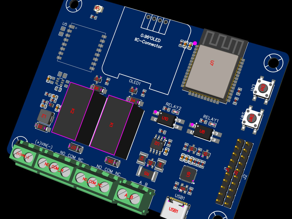
This project involves the design and development of a versatile LoRa-enabled embedded device based on the ESP32 microcontroller, intended for industrial and IoT applications requiring long-range wireless communication and multi-protocol sensor connectivity.
The device operates on a 5V DC power supply and incorporates reverse polarity protection to ensure safe operation and improved hardware reliability in field environments.
The system integrates two onboard I2C display, relays for remote control of external loads and includes a user-configurable switch for manual operation or device interaction. Multiple GPIO pins are exposed to support connection with a wide range of sensors and peripherals using standard communication protocols such as I2C, SPI, and UART, enabling flexible expansion for different monitoring and automation applications.
Additionally, the device features an inbuilt RS485 communication interface, allowing reliable long-distance wired communication suitable for industrial networks and Modbus-based systems.
Key design considerations include robust power management, reliable communication interfaces, modular sensor connectivity.
Materials
Synthetic FibersField of Expertise
IoTDesign Software
OtherFile Format
OtherWhat's included
| Service Tiers |
Starter
$50
|
Standard
$75
|
Advanced
$150
|
|---|---|---|---|
| Delivery Time | 4 days | 6 days | 8 days |
Number of Revisions | 1 | 3 | 4 |
3D Model | - | ||
Source Files |
Optional add-ons
You can add these on the next page.
Additional Revision
+$10
3D Model
+$5
15 reviews
(13)
(1)
(0)
(0)
(1)
This project doesn't have any reviews.
VV
Vishnu V.
Apr 4, 2026
Battery Operated Node with 2 DIgital sensors LED button etc.
“Gaurav did an excellent job. He understood the requirements clearly, communicated well throughout the project, and delivered quality work on time. A pleasure to work with
EC
Eric C.
Jan 14, 2026
Updates to board
PM
Patrizio M.
Dec 13, 2025
PCB Design Review and Fixing
This freelancer is very sloppy and caused a lot of damage to the production. After this freelancer got involved, the PCB designs got compromised and injected with many errors. We lost the entire production, 5 months of work, and had to hire a brand new freelancer to re-design fro scratch. Although freelancer got paid in full, he failed to deliver and (to the contrary) created enormous damage to the project. Wwe would never recommend this freelancer to anyone
SP
Stefan P.
Dec 9, 2025
PCB with RF430FRL152H
DK
Dwarkesh K.
Nov 21, 2025
PCB Design and Gerber File Development
About Gaurav
PCB Design | Embedded Systems | IoT Developer
100%
Job Success
Aligarh, India - 2:20 am local time
Hope you are doing well.
Are you looking to turn your electronic idea into a reliable, compact, and production-ready PCB? You’re in the right place. I help startups, product teams, and businesses design robust hardware that works in the real world — not just on paper.
Why Choose Me?
With 4+ years of hands-on experience in PCB design, firmware development, and prototyping, I’ve successfully delivered consumer, industrial, and IoT hardware projects from concept to working prototype and manufacturing. I understand both engineering fundamentals and production constraints, which helps reduce risk, cost, and redesign cycles.
My core expertise includes:
# PCB Design Tools
EasyEDA/PRO, KiCad, DipTrace
# Microcontrollers & Platforms
ESP32 (S3, C3, C6), STM32, ATmega family & nRF series
# Firmware & Programming
Embedded C/C++, ESP-IDF, Arduino, HAL-based development
# Low-Power & Compact Designs
Battery-operated, wearable, and ultra-small form-factor PCBs
# Wireless & IoT Systems
Wi-Fi, BLE, GSM / LTE / 4G
# Interfaces & Sensors
I²C, UART, USART, SPI, RS485, RS232, CAN
# Power Electronics
Buck converters, LDOs, battery charging & protection, reverse-polarity and ESD protection
What I Offer
# End-to-End Hardware Development
Schematic design, component selection, PCB layout, and design optimization
# Firmware Development & Programming
Peripheral drivers, sensor interfacing, communication stacks, power optimization
# Full Prototype Support
Board bring-up, debugging assistance, validation, and iteration support
# Manufacturing-Ready Designs
DFM/DFA-optimized layouts compatible with JLCPCB / PCBWay
# Production Deliverables
Gerbers, BOM (LCSC-preferred parts), Pick-and-Place, STEP files
# Reliable Power & Protection Design
Low-noise rails, battery optimization, and user-proof protection circuits
Why Clients Love Working With Me
I deliver clean, documented, and review-ready designs
I support projects beyond just files — up to working prototypes
I respect timelines and budgets
I communicate clearly and proactively
I focus on practical, manufacturable solutions
If you’re looking for someone who can design the PCB, write the firmware, and support the prototype until it works, I’d be glad to collaborate.
Let’s connect and build something reliable together.
Steps for completing your project
After purchasing the project, send requirements so Gaurav can start the project.
Delivery time starts when Gaurav receives requirements from you.
Gaurav works on your project following the steps below.
Revisions may occur after the delivery date.
Approve the project detials