You will get Schematic and PCB Design from an idea to product
Project details
I provide professional PCB design and embedded system development services for startups, engineers, and product developers. My focus is on delivering high-quality, production-ready PCB designs that are reliable, efficient, and optimized for real-world performance.
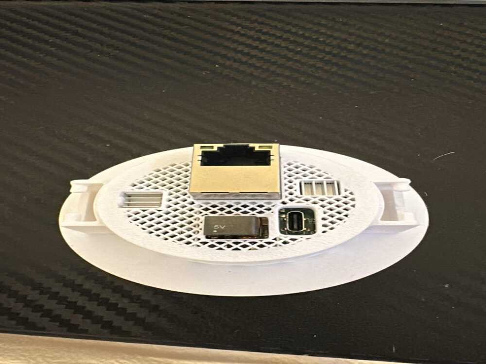
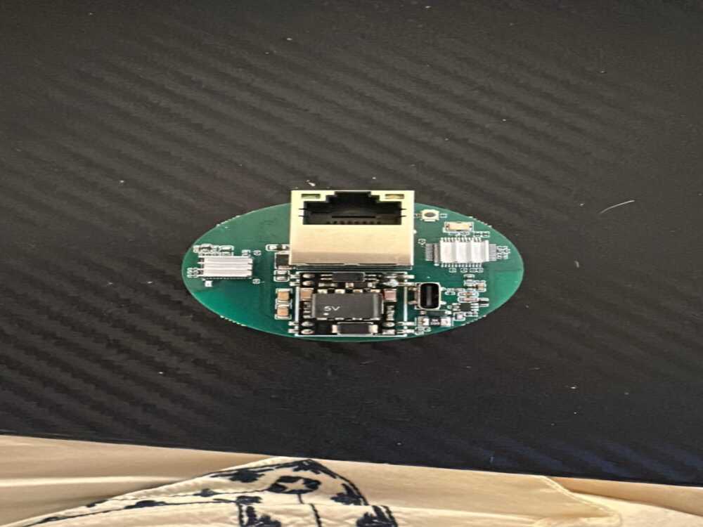
With strong experience in ESP32, IoT systems, power electronics, and multi-layer PCB design, I handle complete development from schematic design to PCB layout, BOM, and manufacturing files (Gerbers, pick-and-place). I carefully consider signal integrity, power distribution, grounding, and component availability (LCSC/JLCPCB) to ensure smooth fabrication and assembly.
What sets me apart is my practical engineering approach. I don’t just design circuits, I design boards that work in real conditions. I have successfully delivered 100+ PCB and embedded projects, including sensor systems, communication devices, and complex integrated boards.
Whether you need a prototype or a production-ready design, I ensure clean layout, accurate documentation, and full support throughout the process helping you reduce errors, save cost, and speed up development.
Materials
OtherField of Expertise
Consumer Electronics, IoT, WearablesDesign Software
OtherFile Format
JPG, PDF, STEP, OtherWhat's included
| Service Tiers |
Starter
$50
|
Standard
$150
|
Advanced
$300
|
|---|---|---|---|
| Delivery Time | 3 days | 7 days | 14 days |
Number of Revisions | 1 | 2 | 3 |
Concept Development | |||
3D Model | - | ||
Source Files |
Frequently asked questions
2 reviews
(1)
(1)
(0)
(0)
(0)
This project doesn't have any reviews.
FR
Fabian R.
May 4, 2026
PCB Layout for ESP32 Sensor Board
Shuja took the work on on very short notice, he worked fast and was knowledgable. The delivered PCBs worked as expected.
AA
Assaf A.
Apr 1, 2026
PCB Design from LTSpice Schematic
Great freelancer
About Shuja
Printed Circuit Board Engineer
100%
Job Success
Islamabad, Pakistan - 1:10 am local time
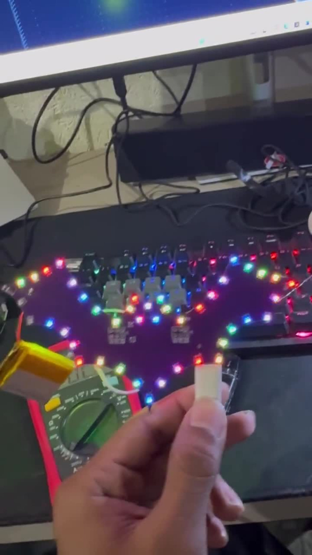
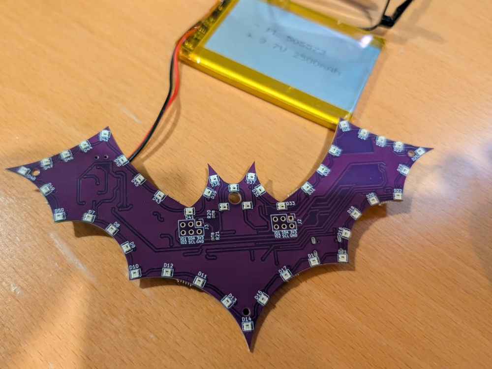
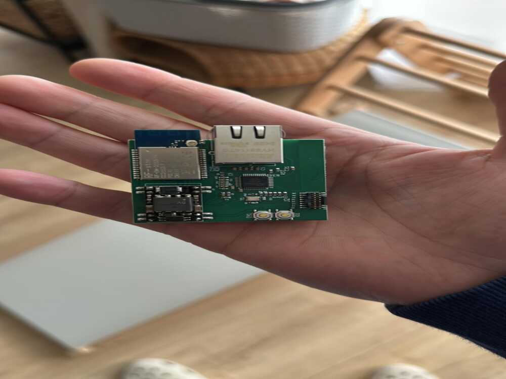
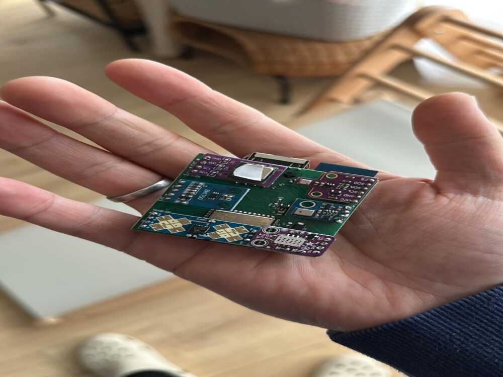
I have hands-on experience designing battery-powered devices with LiPo charging, USB-C interfaces, and efficient power architectures including buck and buck-boost converters. I also work extensively with ESP32, BLE, IoT systems, and addressable RGB LEDs such as WS2812.
My expertise includes schematic design, PCB layout (2-layer to multi-layer), component selection (LCSC/JLCPCB optimized), and hardware debugging. I focus on reliability, clean layouts, and manufacturable designs.
I have successfully delivered complex projects including custom-shaped PCBs, wearable electronics, and embedded systems requiring precise power management and stable performance.
If you are looking for a reliable engineer who can turn your idea into a fully working hardware product, I’m here to help.
Steps for completing your project
After purchasing the project, send requirements so Shuja can start the project.
Delivery time starts when Shuja receives requirements from you.
Shuja works on your project following the steps below.
Revisions may occur after the delivery date.
Review Project Requirements
I will carefully analyze your project details, documents, and technical requirements to fully understand the scope before starting the design process.
Schematic Design & Component Selection
I will design or review the schematic, ensure correct connections, and choose reliable, cost-effective components based on availability and project requirements.